


Lamellar polymer single crystals have been studied since the 1950s, while the potential application of these highly-ordered polymers is much less frequently considered. Recently, Professor Hanying Li and Yuhui Yang from Zhejiang University, China, report, for the first time, the electronic application of the lamellar polymer single crystals for the dielectrics of organic field effect transistors (OFETs). The results show that lamellar polymer single crystals are superior to the widely-used polymer films in the sense that much higher charge mobility is achieved.
Transistors are the fundamental building blocks of electronic devices such as displays, sensors, and complementary circuits. Organic materials have been introduced to build OFETs to make low-cost, flexible, and lightweight devices. OFETs are interface devices where charges transport at the semiconductor/dielectric interface, and the properties of this interface significantly determine the device performance of OFETs.
In principle, ordering of the interfacial structure can enhance OFETs performance. Single crystals are ideal candidates for high-performance OFETs due to the ordered molecular packing. As such, single crystals of semiconductors are quite often used for OFETs and high-performance OFETs are achieved. Interestingly, using single crystals in the dielectric side of the semiconductor/dielectric interface is much less frequently considered.
Only in a few cases, were single crystals of mica and organic small molecules used as dielectrics for OFETs by Ueno group (Chem. Lett. 2006, 35, 354-355), Takeya group (Solid-State Electron. 2007, 51, 1338-1343), and Hu group (Adv. Mater. 2011, 23, 5502-5507; Adv. Mater. 2016, 28, 3755-3760). Especially, for the polymer materials that have been widely used as dielectrics in OFETs, the single-crystalline form has not been adopted for OFETs.
Ideally, a semiconductor/dielectric interface with single-crystalline materials on both sides (i.e., single-crystalline semiconductors and single-crystalline dielectrics) is highly desired to favor the electron transport along the interface. Professor Hanying Li and Yuhui Yang reported this kind of highly ordered interface where Poly(ε-caprolactone) (PCL) single crystal was chosen as the dielectric side while 6,13-bis(triisopropylsilylethynyl)-pentacene (TIPS-pentacene) single crystal as the semiconductor side. The fabrication process of OFETs is shown in Figure 1.
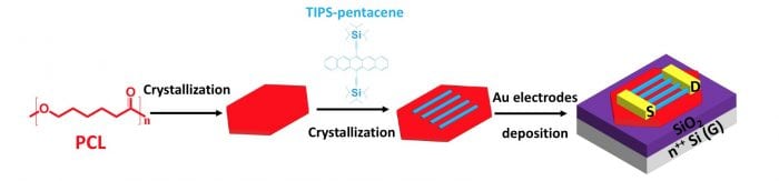
Figure 1. Schematic illustrates the fabrication process of OFETs with PCL single crystal as dielectrics and TIPS-pentacene single crystal as semiconductors. PCL single crystals were grown in dilute 1-butanol solution by the self-seeding method, and TIPS-pentacene single crystals were grown via the droplet-pinned crystallization (DPC) method. (Republished with permission from Polymer)
Obtaining large size and smooth polymer single crystals is the key to the preparation of polymer single crystal dielectrics for OFETs. PCL has been shown to easily form lamellar single crystals with flat crystalline terrace using the self-seeding method but their sizes were too small for OFETs. In order to fabricate OFETs on PCL single crystals, the large size (up to 83 μm in length) PCL single crystals with a smooth surface were obtained by reducing the nucleus density in the process of crystallization (as shown in Figure 2a-c).
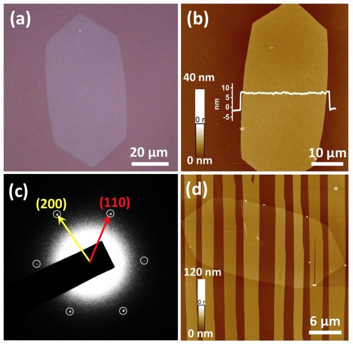
Figure 2. Morphologies and crystalline structures of PCL single crystals and bilayer single crystals. (a) An optical microscopy image of PCL single crystal. (b) An atomic force microscopy (AFM) image of a PCL single crystal. The inset curves show the height profile of the corresponding PCL crystal lamellae. (c) A selected area electron diffraction pattern of a PCL single crystal with the white circles highlighting the diffraction spots, showing the single-crystallinity. (d) An AFM image of bilayer single crystals with TIPS-pentacene ribbons on top of PCL lamellae. (Republished with permission from Polymer)
Next, crystallization of TIPS-pentacene on the PCL single crystal forms the interface for electron transport in OFETs (as shown in Figure 2d). The devices exhibit hole mobility as high as 4.95 cm2V-1s-1 (average mobility: 1.70±0.97 cm2V-1s-1). The mobility is much higher than that of the devices based on the relatively disordered PCL thin films (average mobility: 0.62±0.24 cm2V-1s-1), indicating the advantage of polymer single crystalline dielectrics. As such, this result demonstrates that single-crystalline polymer dielectrics are promising for high-performance OFET devices.
These findings are described in the article entitled Polymer Single Crystal Dielectrics for Organic Field-Effect Transistors, recently published in the journal Polymer. This work was led by Hanying Li, Yuhui Yang, and Hongzheng Chen from Zhejiang University.
Related Posts
 Improving Tools For Quality Improvement: Crossings, Runs, And Crossrun
 Coherent Poly Propagation Materials With 3-Dimensional Photonic Control Over Visible Light
 Reconstructing Commuter Networks Using Machine Learning And Urban Indicators
 Surprising Internal Structure Of Whole Wheat-Green Gram Functional Bread
 Tailoring Tomatoes To Match Individual Consumer Needs
 Eavesdropping On “Classroom Talk” In Undergraduate STEM Classrooms