


The retinal visual system of mammals is regarded as an ideal imaging system due to its wide field of view (FOV), low aberration, and low f-number. The simple one-lens imaging system is enabled by the curved retina located at the back of the eyeball.
Compared to the natural imaging system, most of the modern artificial imaging systems are based on flat focal plane array (FPA) technology. The planar FPA system requires complicated multi-element lenses to correct the radial image surface, as known as Petzval surface, to be flattened so the optical aberrations can be removed. However, the complex lens system has been a major bottleneck to develop more compact and high-performance imager for the next-generation camera system.
If a camera system can have a curved image surface mimicking a spherical retina of primates, it can provide numerous advantages such as wide field of view, less optical errors, and less optical lens components, which can lead to the development of cheaper and lighter camera system. However, making the sensor array in a curved surface has been regarded as challenging technology due to the difficulty of the development of unconventional fabrication method.
Recently, Prof. Jerzy Kanicki and his co-workers at the University of Michigan, EECS Department developed a facile method to enable the organic photo-sensor array on a hemispherical surface. To achieve the goal, they developed a novel way to fabricate a curved shadow mask by three dimensional (3D) printing technology for the electrode patterning of the array. Moreover, a newly developed transfer printing method, called Double Transfer Stamping (DTS), by the same group (published in Advanced Optical Materials) [1] has been used to provide a degree of freedom to organic photoactive layer formation, which features a 3D-shaped elastomeric polydimethylsiloxane (PDMS) stamps.
Both 3D printed shadow mask and DTS method allowed the direct patterning of the organic photo-sensor arrays on the concavely curved substrates without any excessive strain or deformation. The photodiode adapted dielectric / thin metal / dielectric top transparent electrode structure (published in Organic Electronics) [2] was used to allow the top absorption of the incident light. The fabricated organic photodiode passive arrays on a hemispherical substrate with FOV = 120o showed high performance with detectivity of 1.4 x 10¹¹ Jones at a green light wavelength.
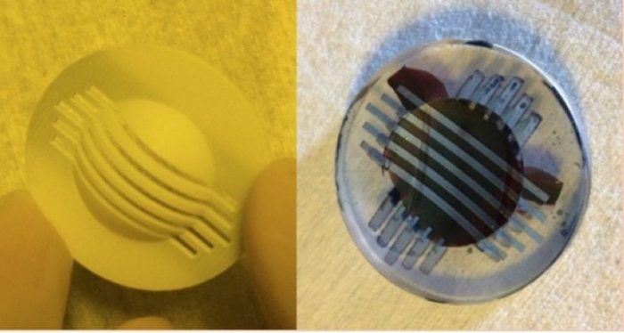
3D printed shadow mask and fabricated hemispherical organic photodiode array. Credit: Jerzy Kanicki’s lab
The team believes that the developed 3D mask and 3D organic layer transfer printing process can be further utilized for various optoelectronic device applications which necessitate a free form factor on arbitrary substrates. Particularly, the hemispherical sensor array can be combined with the metal oxide thin-film transistor active-matrix arrays (published in IEEE Transaction on Electron Devices) [3], developed by the same group, to allow the fabrication of the novel imaging systems on curved substrates such as artificial human eyes or X-ray imagers for breast cancer detection [5], eventually opening new business opportunities for more compact, high performance image sensing devices.
References
- H. Kim, B. Song, K. Lee, S. Forrest and J. Kanicki, Advanced Optical Materials, 2017, 1600784
- H. Kim, K.-T. Lee, C. Zhao, L.J. Guo and J. Kanicki, Organic Electronics, 20 (2015) 103-111
- M.-H. Cheng, C. Zhao, C.-L. Huang, H. Kim, NM. Nakata and J. Kanicki, IEEE Transaction on Electron Devices, 6 (2016) 4802-4810
- H. Kim, J. Moon, K. Lee and J. Kanicki, Advanced Materials Technologies, 2017, 2, 1700090
- C. Zhao and J. Kanicki, Medical Physics, 49 (2014) 091902
This study, 3D Printed Masks and Transfer Stamping Process to Enable the Fabrication of the Hemispherical Organic Photodiodes was recently published in Advanced Materials Technologies.
Related Posts
 Improving Tools For Quality Improvement: Crossings, Runs, And Crossrun
 Coherent Poly Propagation Materials With 3-Dimensional Photonic Control Over Visible Light
 Reconstructing Commuter Networks Using Machine Learning And Urban Indicators
 Surprising Internal Structure Of Whole Wheat-Green Gram Functional Bread
 Tailoring Tomatoes To Match Individual Consumer Needs
 Eavesdropping On “Classroom Talk” In Undergraduate STEM Classrooms